Semiconductors
The semiconductor industry melts, dopes, deposits, and anneals silicon and other semiconductor materials to make the building blocks of electronic circuits. All of these processes require temperature monitoring and control. Contact temperature measurement techniques are not desirable because such methods can affect the temperature of the sample or contaminate it with the material of the contact sensor. Additional contraindications are that small (low thermal mass) or moving targets are difficult for contact techniques. Unfortunately, semiconductor materials also make notoriously difficult non-contact temperature measurement targets. The emissivity of silicon illustrates this:
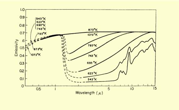
Emissivity of silicon as a function of temperature and wavelength, from Sato, T., Jap. J. Appl. Phys. 6, March, 1967, p. 339-347.
The SpectroPyrometer has successfully measured the temperature of a moving silicon wafer during annealing. One set of optics was sequentially shared by an FMPI and an FMP2 SpectroPyrometer, sensitive to 1000 – 1700 nanometers and 500 – 1000 nanometers, respectively. Both instruments were successful in returning temperatures with small tolerances, although both faced challenges. The FMP2 had to contend with a helium-neon laser line superimposed on the thermal spectrum; the FMPI detected emissivity changing with wavelength after the 1100 nm bandgap.
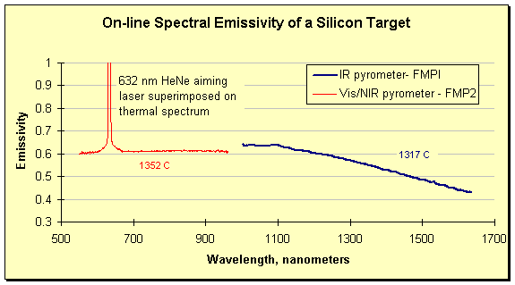
On-line spectral emissivity of a silicon wafer undergoing annealing, as measured by two different SpectroPyrometers. Temperatures for the two spectra are different because the two instruments sequentially shared one set of optics and therefore measured at different stages of processing.